Part 16 told the story of the GPU as Nvidia's story, and for the AI era that is mostly fair. But for most of the time Nvidia has existed it had a rival of roughly its own size, and for some stretches the rival had the better chip. That rival was ATI, a Canadian company that AMD bought in 2006, and its descendants are the Radeon cards that have been Nvidia's only lasting competition in gaming PCs, the graphics in every PlayStation and Xbox since 2013, two of the three fastest supercomputers on the most recent list, and the GPUs that OpenAI, Meta and Anthropic have signed gigawatt-scale contracts to buy. This part is that story, told the same way as Part 16, with the chips that changed something and the eras they fall into.
Era one: ATI against Nvidia (1985 to 2006)
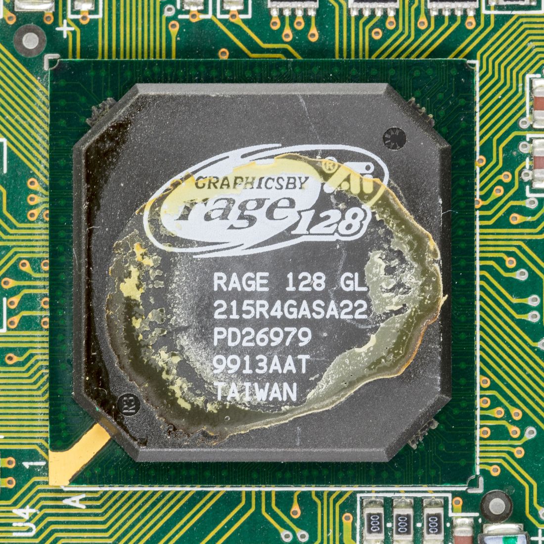
ATI was founded in August 1985 in Markham, Ontario, outside Toronto, by Kwok Yuen Ho, Lee Ka Lau and Benny Lau, under the name Array Technology, and it spent its first decade making the cards that let a PC show anything at all: the Wonder series, then the Mach chips that accelerated the drawing of windows and text, then from 1996 the Rage line, which added 3D. The first chip called Radeon arrived in 2000. That same year ATI bought ArtX, a small Silicon Valley company founded by former Silicon Graphics engineers, which had just designed the graphics chip for Nintendo's GameCube. The purchase brought in Dave Orton, who became ATI's president, and a design team that would matter more than anything else ATI bought.
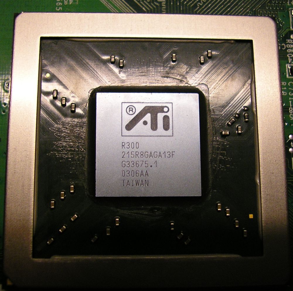
That team's first big chip for ATI was the R300, sold as the Radeon 9700 Pro from the summer of 2002. It was the first graphics chip to support everything in Microsoft's DirectX 9, the version that made pixel shaders programmable with real floating-point arithmetic, and it had a 256-bit memory bus, twice the width of Nvidia's. About 110 million transistors on a 150 nm process. Nvidia's answer, the GeForce FX 5800, arrived several months late in early 2003 and lost most of the comparisons that mattered. It was the clearest win ATI ever had: for the better part of two years, the fastest graphics chip you could buy was not an Nvidia one.
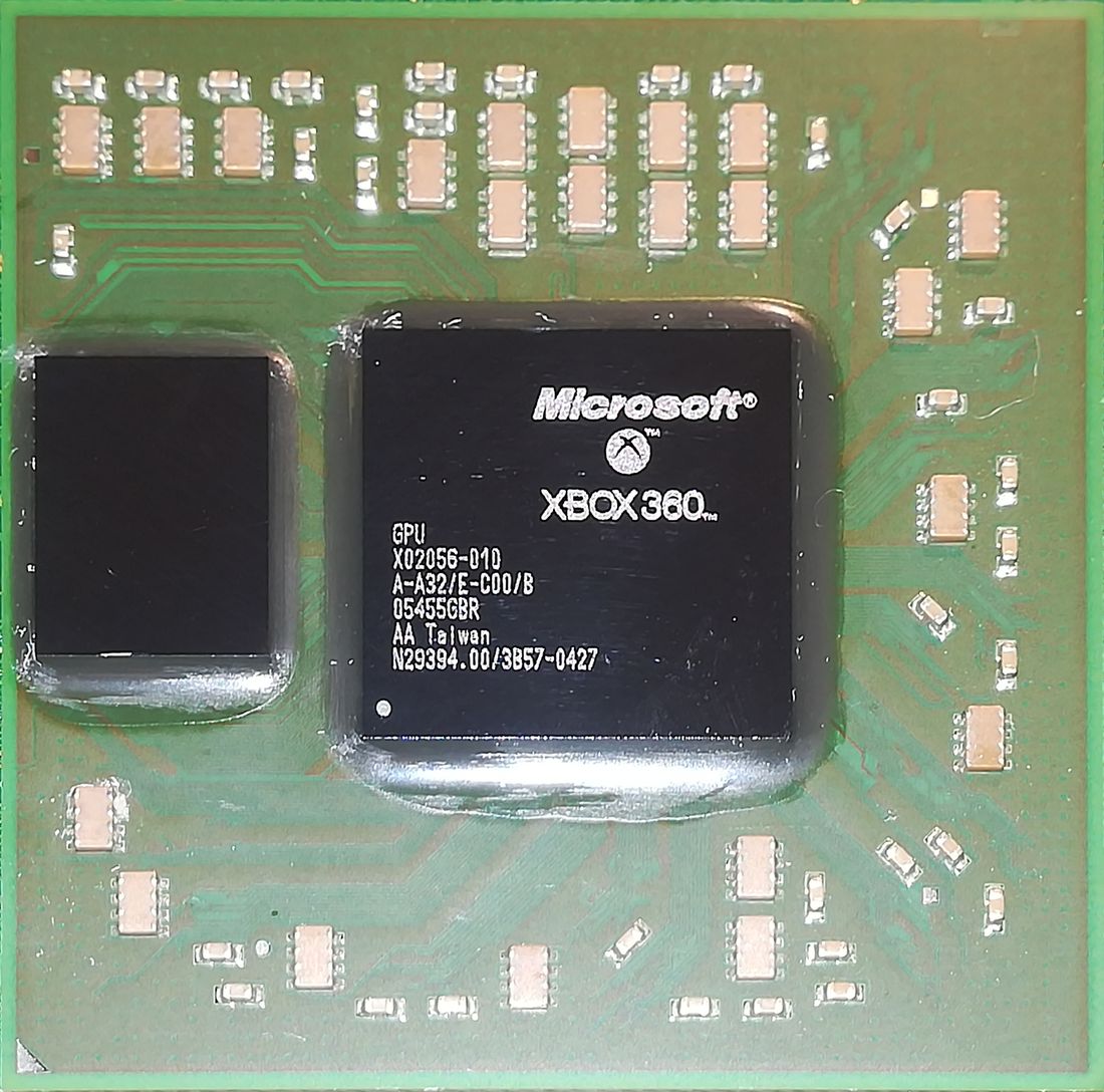
The other thing ATI did in this era was win the consoles. ArtX's GameCube chip became ATI's, its successor went into Nintendo's Wii, and for Microsoft's Xbox 360, launched in November 2005, ATI built Xenos. Xenos had 48 arithmetic units that could each do either vertex work or pixel work, scheduled as the frame demanded, which is the unified shader idea that Part 16 credits to Nvidia's G80. Xenos shipped it a full year earlier, in a games console rather than a PC. It also carried 10 MB of fast embedded memory on a second die in the same package, a small early instance of an idea AMD would return to at enormous scale: put the memory the arithmetic needs most right next to it.
Era two: the takeover and the small die (2006 to 2011)
In July 2006 AMD, then Intel's only competitor in PC processors, agreed to buy ATI, and completed the purchase that October for about $5.4 billion in cash and shares. The idea was a company that could put a processor and a graphics chip on one piece of silicon, which AMD would eventually do very well. The timing was terrible. The deal loaded AMD with debt just as Intel's Core 2 processors overtook AMD's, and within two years AMD had written off more than $2.4 billion of what it had paid. The graphics side did not help at first. ATI's first PC chip with unified shaders, the R600 in the Radeon HD 2900 XT of May 2007, came out six months after the G80, used more power, and could only be priced against Nvidia's second-tier card.
What saved AMD's graphics was a decision taken in 2005, before the takeover: stop trying to build the biggest chip, and build the best one for the price people actually pay. The RV770, in the Radeon HD 4870 and 4850 of June 2008, was the result. It had 800 stream processors and 956 million transistors on a die of about 256 mm². Nvidia's flagship that summer, the GT200 in the GeForce GTX 280, had 1.4 billion transistors on about 576 mm² and launched at $649. The HD 4870 cost $299, came within reach of it in many games, and was the first graphics card to use GDDR5 memory. AnandTech called it the small-die strategy, and for a few years it worked: make a mid-sized chip on the newest process, sell it at the price where most cards are bought, and put two of them on one board for the top of the market.
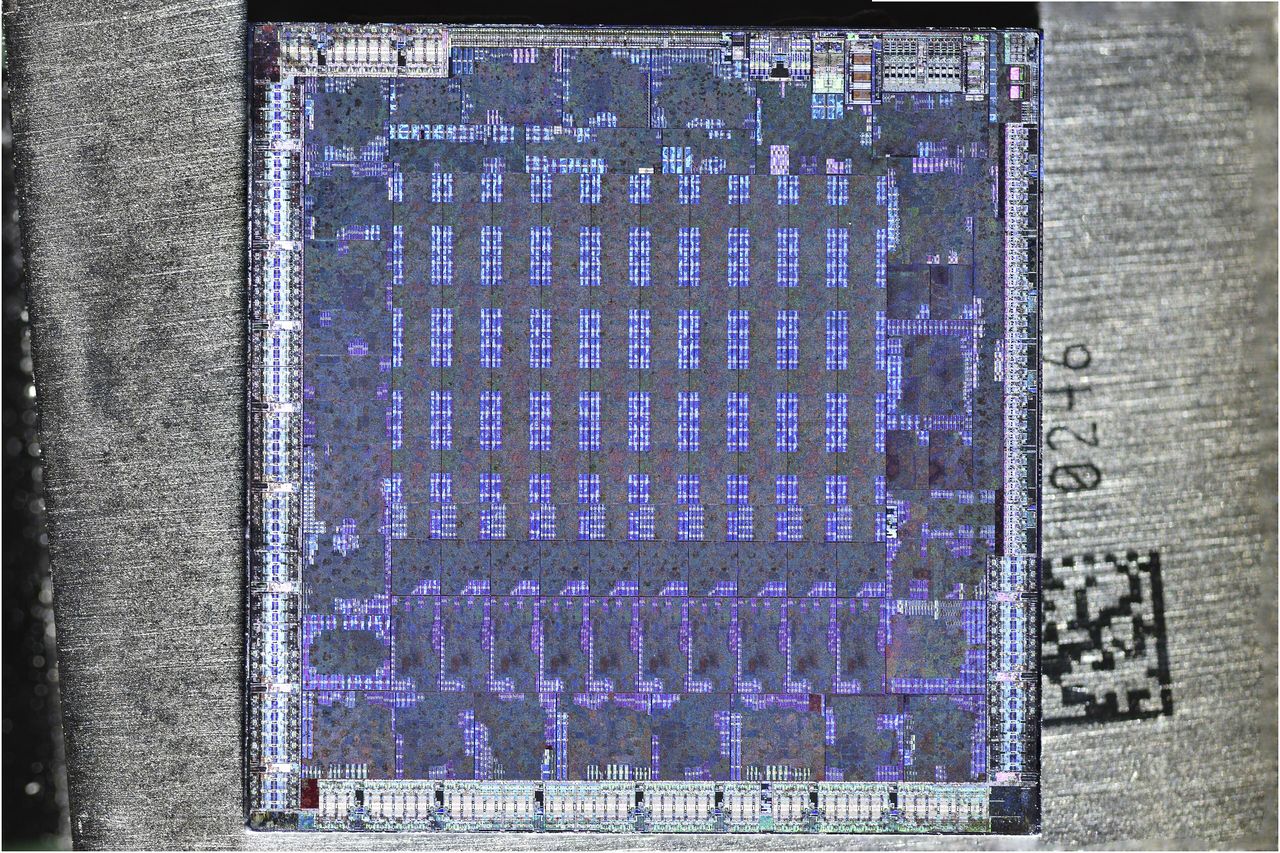
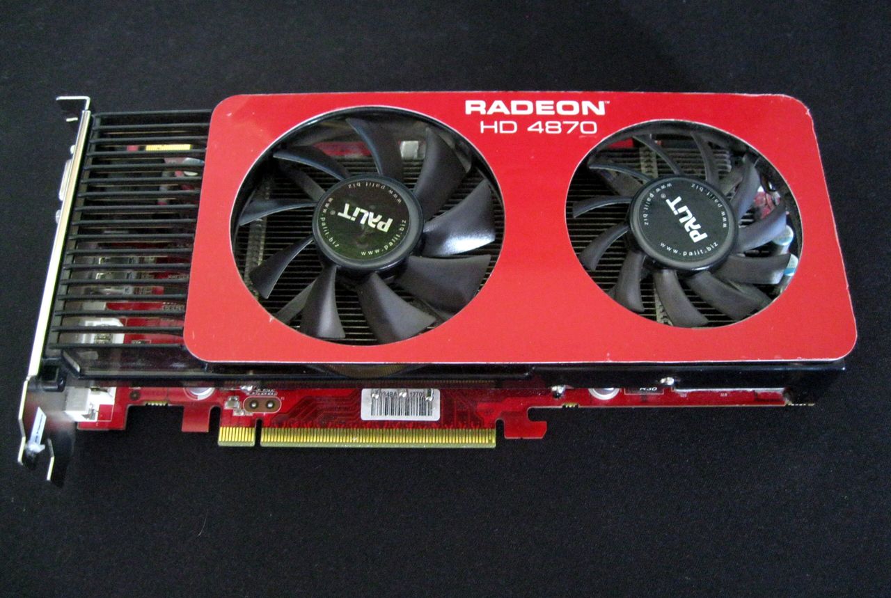
The Radeon HD 5870 of September 2009 was the first graphics card for DirectX 11, with 2.15 billion transistors and 1,600 stream processors on 40 nm, and once again it arrived months before Nvidia's equivalent, Fermi. But underneath, these chips all shared the very-long-instruction design that Part 10's side note described: lanes of four or five arithmetic units each, kept busy only if the compiler found that many independent operations in one thread. For games that worked. For the general-purpose computing that CUDA had made popular on Nvidia's side, it did not, and the gap in software that opened in these years, CUDA in 2007 against a succession of AMD efforts, Close to Metal, the Stream SDK and then OpenCL, none of which built the same following, is the one AMD is still closing.
Era three: GCN and the lean years (2012 to 2018)
The fix for the hardware side was Graphics Core Next, which arrived in the Radeon HD 7970 in January 2012 and is the compute unit of Part 10: one simple operation per lane, wavefronts of 64, a scalar unit, the same bet Nvidia had made in 2006. GCN was a good design and became an unusually long-lived one, because of a contract signed around the same time. Sony's PlayStation 4 and Microsoft's Xbox One, both launched in November 2013, used AMD processors with GCN graphics on the same chip, the combined chip AMD had bought ATI to make. Every PlayStation and every Xbox since has used AMD graphics, and that steady business is a large part of how Radeon survived the next five years.
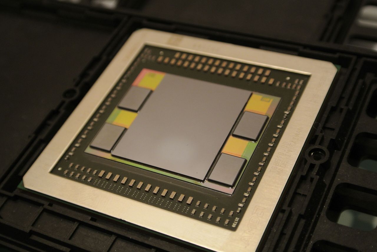
It needed to. AMD's processors fell far behind Intel's, its finances with them, and in 2015 its shares traded for under two dollars. Lisa Su, an engineer who had joined AMD in 2012, became chief executive in October 2014, and in September 2015 the graphics teams were gathered into a Radeon Technologies Group under Raja Koduri. The chips of these years were inventive and constrained. Fiji, in the Radeon R9 Fury X of June 2015, was the first GPU with HBM, the stacked memory of Part 12, developed with SK hynix: four stacks beside the die on a silicon interposer, a 4,096-bit memory bus, a year before Nvidia's first HBM chip. Polaris in 2016 was a $199 card aimed squarely at the middle of the market. Vega in 2017 brought HBM2 and 12.5 billion transistors, and its 7 nm successor became, in November 2018, the first 7 nm GPU of any kind, sold as the Instinct MI60 and MI50 for data centres and the Radeon VII for games.
The software started in these years too. In November 2015 AMD announced what it called the Boltzmann Initiative, with a Linux driver built for computing and a language called HIP designed to look almost exactly like CUDA, and in 2016 those became the first release of ROCm, AMD's answer to the CUDA stack of Part 14. The Radeon Instinct line of data-centre cards followed in 2017. Neither made much of a dent at first. Nvidia had a ten-year head start, and in 2017 Volta added tensor cores, which no AMD chip would have for another three years.
Era four: two architectures and the supercomputers (2019 onward)
In 2019 AMD redesigned its GPU for graphics as RDNA, and in 2020 it split the line in two, as Part 10 explained: RDNA for games and consoles, CDNA for computing, starting with the Instinct MI100 and its first matrix cores. RDNA 2 went into the PlayStation 5 and the Xbox Series X and S in November 2020, and into Valve's Steam Deck in 2022.
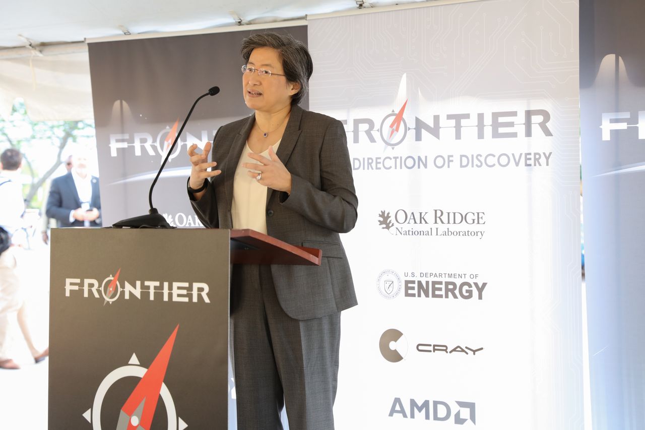
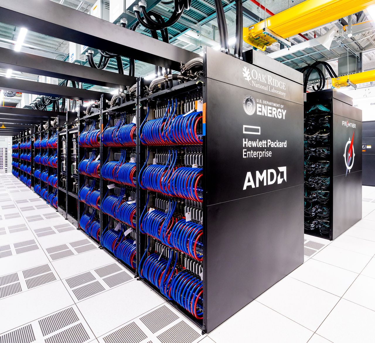
The data-centre line found its first big customer not in AI but in supercomputing. In May 2019 the US Department of Energy announced that Oak Ridge National Laboratory's next machine, Frontier, would be built by Cray with AMD processors and AMD GPUs. The GPU it ended up with was the MI250X of 2021, the first AMD product with two GPU dies in one package, and in May 2022 Frontier became the first computer to pass an exaflop on the standard benchmark, a billion billion operations a second at 64-bit precision, with 37,632 MI250X GPUs. Its successor at Lawrence Livermore, El Capitan, built on the MI300A, took the top place in November 2024. On the June 2026 list a new Chinese system, LineShine, built without GPUs at all, moved ahead of both, and El Capitan and Frontier stand second and third.
The chips of this era are the subject of the rest of this series, so here they are in a sentence each. RDNA 3, in the Radeon RX 7900 XTX of December 2022, was the first gaming GPU built from chiplets, and RDNA 4, in the RX 9070 XT of 2025, went back to a single die (Part 22). The MI300X of December 2023 stacked eight compute dies on four base dies with 192 GB of memory, more than twice the H100's, and became AMD's first real success in AI (Part 25). The MI355X of June 2025 took the same design to 3 nm and 4-bit arithmetic (Part 28). And the MI455X of July 2026, in a rack of 72 called Helios, is AMD's first machine built as a rack from the start (Part 30).
Around the chips, AMD bought what Nvidia had built for itself. It bought the FPGA maker Xilinx in 2022, the networking-chip company Pensando the same year, a string of AI software companies from 2023 onward, and in 2025 ZT Systems, a maker of server racks, for $4.9 billion, keeping its design engineers and selling its factories on to Sanmina. The money came with it. AMD's Instinct GPUs earned more than $5 billion in 2024, their first big year, and data-centre revenue, CPUs and GPUs together, reached $6.7 billion in the second quarter of 2026 alone. The contracts are larger still. In October 2025 OpenAI agreed to deploy six gigawatts of AMD GPUs over several years, starting with the MI450 generation in the second half of 2026, and AMD gave it warrants for up to 160 million AMD shares that vest as the deployments happen. Meta signed a deal of the same size and shape in February 2026, and Anthropic one for up to two gigawatts in July 2026. Meanwhile, on the side of the business where it all began, AMD's share of desktop graphics cards fell to between 5 and 8 per cent in 2025 and 2026 by Jon Peddie Research's count.
The whole run in one table
| Architecture | Year | Flagship | Transistors | Process | What it added |
|---|---|---|---|---|---|
| R300 | 2002 | Radeon 9700 Pro | 0.11 billion | 150 nm | first full DirectX 9 chip, 256-bit bus |
| Xenos | 2005 | Xbox 360 | 0.23 billion, plus a memory die | 90 nm | unified shaders, embedded memory |
| TeraScale (R600) | 2007 | Radeon HD 2900 XT | 0.70 billion | 80 nm | unified shaders on a PC, VLIW5 |
| RV770 | 2008 | Radeon HD 4870 | 0.96 billion | 55 nm | the small-die strategy, first GDDR5 |
| Cypress | 2009 | Radeon HD 5870 | 2.15 billion | 40 nm | first DirectX 11 chip |
| GCN (Tahiti) | 2012 | Radeon HD 7970 | 4.3 billion | 28 nm | the compute unit, the scalar unit |
| Fiji | 2015 | Radeon R9 Fury X | 8.9 billion | 28 nm | first HBM, silicon interposer |
| Vega 20 | 2018 | Instinct MI60 | 13.2 billion | 7 nm | first 7 nm GPU |
| RDNA (Navi 10) | 2019 | Radeon RX 5700 XT | 10.3 billion | 7 nm | wave32, work-group processors |
| RDNA 2 (Navi 21) | 2020 | Radeon RX 6900 XT | 26.8 billion | 7 nm | Infinity Cache, ray tracing |
| CDNA 2 (MI250X) | 2021 | Instinct MI250X | 58 billion, 2 dies | 6 nm | two dies per package, FP64 matrix cores |
| RDNA 3 (Navi 31) | 2022 | Radeon RX 7900 XTX | 58 billion, 7 dies | 5 and 6 nm | the chiplet gaming GPU |
| CDNA 3 (MI300X) | 2023 | Instinct MI300X | 153 billion, 12 dies | 5 and 6 nm | stacked chiplets, 192 GB of HBM3 |
| RDNA 4 (Navi 48) | 2025 | Radeon RX 9070 XT | 53.9 billion | 4 nm | FP8 on a gaming card, back to one die |
| CDNA 4 (MI355X) | 2025 | Instinct MI355X | 185 billion | 3 and 6 nm | FP4 and FP6, 288 GB |
| CDNA 5 (MI455X) | 2026 | Instinct MI455X | 320 billion | 2 and 3 nm | wave32 for compute, HBM4, the 72-GPU rack |
What the history is telling you
Three things stand out when you set this beside Part 16.
The first is how often ATI and AMD got to the hardware idea first. Unified shaders in a console a year before the G80. GDDR5, then HBM a year before Nvidia, then the first 7 nm GPU, then two dies in one package in 2021, chiplets in a gaming card and stacked chiplets in a data-centre one, all before Nvidia joined two dies together. Being first was never the problem. What Nvidia had and AMD did not was the software and the patience: CUDA in 2007 and kept stable ever since, against an AMD that changed its compute strategy several times and did not ship ROCm until 2016. Part 16 said that Nvidia's advantage was making a general machine and then keeping the software stable for two decades. This history is the same lesson from the other side.
The second is that AMD's graphics survived on the products that do not make headlines. The small-die chips of 2008, the console contracts of 2013 onward, and the national laboratory supercomputers from 2019 kept the Radeon and Instinct lines funded through years when AMD could not afford to build the biggest chip, and the supercomputers paid for the packaging and chiplet work that the MI300X was built on. The AI customers arrived after the hardware was ready, not before.
The third is the shape of the curve. AMD's transistor count left the single die behind in 2021, with two dies in the MI250X, and has grown since by adding pieces of silicon, not by enlarging them: twelve logic dies in the MI300X, and twelve again in the MI455X, which uses them to hold 320 billion transistors. That is the reticle wall of Part 3 answered three years before Nvidia answered it with Blackwell, and Part 19, on how a chip is made, is where the yield arithmetic behind that choice comes from. First, the third company, whose relationship with graphics is the oddest of the three.
Next: Intel and Graphics: the company that has shipped more GPUs than anyone and spent a quarter of a century trying to build a big one, from the i740 and Larrabee to Arc, Aurora, Gaudi and the retrenchment of 2025 and 2026.