Part 27 showed Nvidia getting past the reticle wall by joining two big dies. AMD had been past it since 2021, so its 2025 chip did not need a new idea about packaging. It needed more arithmetic per square millimetre, the new four-bit formats, and more memory, and it got all three by keeping the MI300's design and changing almost every number in it. AMD announced the MI350X and MI355X on 12 June 2025 and said they were already shipping to customers. They are the same chip at two power levels, built on an architecture AMD calls CDNA 4.
By the numbers
| MI300X (CDNA 3) | MI355X (CDNA 4) | B200 (Blackwell) | GB200, per GPU | |
|---|---|---|---|---|
| Launched | December 2023 | June 2025 | 2024 | 2024 to 2025 |
| Transistors | 153 billion | 185 billion | 208 billion | 208 billion |
| Silicon | 8 compute dies (5 nm) on 4 base dies (6 nm) | 8 compute dies (3 nm) on 2 base dies (6 nm) | 2 dies (4 nm) | 2 dies (4 nm) |
| Compute units or SMs | 304 CUs | 256 CUs | not published | not published |
| Memory | 192 GB HBM3 | 288 GB HBM3E | 180 GB HBM3E | 186 GB HBM3E |
| Bandwidth | 5.3 TB/s | 8 TB/s | 8 TB/s | 8 TB/s |
| FP16 matrix, dense | 1.3 PFLOPS | 2.5 PFLOPS | 2.25 PFLOPS | 2.5 PFLOPS |
| FP8, dense | 2.6 PFLOPS | 5 PFLOPS | 4.5 PFLOPS | 5 PFLOPS |
| FP6, dense | none | 10 PFLOPS | 4.5 PFLOPS | 5 PFLOPS |
| FP4, dense | none | 10 PFLOPS | 9 PFLOPS | 10 PFLOPS |
| FP64 matrix | 163 TFLOPS | 79 TFLOPS | 37 TFLOPS | 40 TFLOPS |
| GPU-to-GPU links | 896 GB/s, 8 GPUs, no switch | 1,075 GB/s, 8 GPUs, no switch | NVLink 5, 1.8 TB/s, 8 GPUs | NVLink 5, 1.8 TB/s, 72 GPUs |
| Power | 750 W | 1,400 W, liquid-cooled | about 1,000 W | about 1,200 W |
The Nvidia figures are dense values derived from Nvidia's published tables, which list them with sparsity. Read across the MI355X and GB200 columns and the paper numbers are almost the same chip: the same bandwidth, the same FP16, FP8 and FP4 rates to within a rounding error. The differences are in three rows. The MI355X has half as much memory again, it runs six-bit numbers as fast as four-bit ones, and its links join eight GPUs where the GB200's join seventy-two.
Eight compute dies on two
The package keeps Part 10's plan, stacked compute dies on base dies with HBM around them, and changes the proportions. The eight accelerator complex dies moved from 5 nm to TSMC's 3 nm-class N3P process, each about 110 mm², with 36 compute units of which 32 are switched on, the usual margin for defects. The four base dies became two, each carrying four compute dies, which AMD says simplified the Infinity Fabric network between them, cut its latency and saved power. The 256 MB of Infinity Cache stayed. The memory went to eight stacks of HBM3E, each twelve dies high, 36 GB a stack, 288 GB at 8 TB/s.
Notice that the chip has fewer compute units than the one before it. AMD spent the shrink not on more of them but on making each one do more, which is the story of the next section.
A compute unit rebalanced
Part 10 gave the CDNA 3 compute unit's work per clock: 2,048 FP16 operations on its matrix cores, 4,096 at FP8, 256 at FP64. CDNA 4 doubles the matrix rate for 16-bit and 8-bit numbers, adds the new six-bit and four-bit formats at 16,384 operations per clock, and halves the 64-bit matrix rate. Multiply out and you get the headline: 256 compute units, times 16,384 four-bit operations, times 2.4 GHz, is 10 PFLOPS.
Three smaller changes say as much about what the chip is for. The local data share, the scratchpad of Part 10, grew from 64 KB to 160 KB per compute unit, with twice the read bandwidth, so that each compute unit can hold bigger tiles of the matrices it is multiplying, the reuse trick of Part 12. The rate of transcendental functions, the exponentials that the softmax in a transformer's attention needs, doubled. And the TF32 format, a 19-bit compromise that Nvidia introduced with Ampere for training, was dropped from the hardware; CDNA 4 imitates it in software with BF16 when a program asks for it. None of these helps a weather model. All of them help a language model.
Six bits at the price of four
Part 27 explained the four-bit formats and the scale factors that make them usable, and named the industry's version, the MX formats, which give every block of 32 numbers a shared power-of-two scale. CDNA 4 supports MXFP4 and two six-bit variants, MXFP6 with either two exponent bits and three mantissa bits or three and two. On the MI355X, six-bit arithmetic runs at exactly the four-bit rate, 10 PFLOPS. On Blackwell it runs at the eight-bit rate, half that.
Why would anyone want six bits? Because four is often not quite enough. A model whose accuracy suffers at FP4, some layers of it or all of it, can drop to FP6 instead of FP8 and, on this chip, keep the full four-bit arithmetic speed while gaining two bits of precision per number. The catch is the one Part 12 would point to. A six-bit number still takes half as many bytes again to move as a four-bit one, and when a model is generating text the speed limit is bytes, not arithmetic. So FP6 at FP4's rate is a real gain for prompt reading, which is compute-bound, and a smaller one for generation, which is not.
The trade with science
The halved FP64 is worth a moment, because it shows which customers AMD now designs for. The MI300X did 163 TFLOPS of 64-bit matrix arithmetic, which is what made the MI250X and MI300A the supercomputer chips of Part 25. The MI355X does 79, vector and matrix alike, half its predecessor's. Nvidia made the same trade in the same generation, from 67 TFLOPS on the H100 to about 40 on the GB200. Both companies decided that the transistors were worth more spent on four-bit arithmetic for AI than on 64-bit arithmetic for simulation.
AMD's way out is a separate chip. The MI430X, due in 2027 from the MI400 family of Part 30, swaps in compute dies built for FP64 and is promised at 288 TFLOPS of it, for the next generation of national laboratory machines. The split of Part 10, one design for graphics and one for computing, has started to split again inside computing.
Two power levels
The MI350X and MI355X are the same silicon. The MI350X runs at up to 2.2 GHz within 1,000 W and can be air-cooled. The MI355X runs at up to 2.4 GHz within 1,400 W and needs liquid cooling, with cold plates on every GPU like the Blackwell racks of Part 27. On paper the difference is about 8 per cent; AMD told The Register the gap in real workloads is closer to 20 per cent, presumably because the extra power lets the chip hold its top clock for longer under load.
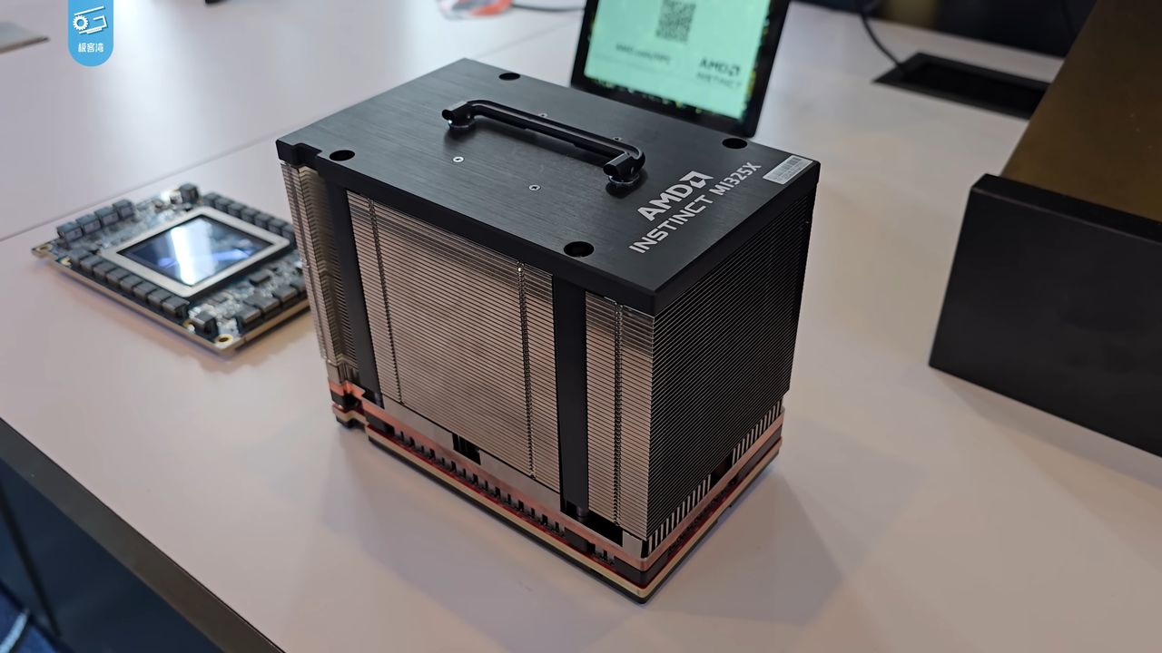
Both still come eight to a server, on the same eight-GPU board as the MI300X, wired each to each with no switch, now at 1,075 GB/s per GPU. AMD sells racks of up to 64 air-cooled MI350X or up to 128 liquid-cooled MI355X, sixteen eight-GPU servers in a rack AMD says needs about 200 kW. That is 128 GPUs in one rack, more than Nvidia's 72, but they are sixteen islands of eight joined by Ethernet, not one domain where every GPU reaches every other at full speed. For the training and the very large models that the 72-GPU NVLink domain of Part 27 was built for, that is the gap, and Helios is AMD's attempt to close it.
Against Blackwell
Spec sheets aside, the most comparable public measurement is MLPerf, the industry benchmark of Part 25. In the round published in April 2026, an eight-GPU MI355X server ran Llama 2 70B at about 103,000 tokens a second offline and 100,000 in the server scenario, which AMD said matched an eight-GPU B200 system offline and came to between 92 and 104 per cent of the newer B300 depending on the scenario. Those are AMD's comparisons of its own submission against Nvidia's, on one model, but they are measured under the same rules, which is more than most claims in this business are.
AMD's launch claims need more care. "Up to 35 times the inference performance of the MI300X" compared the MI355X running at FP4 with a batch of 64 requests against the MI300X at FP8 serving one request at a time, which measures the format and the batching as much as the chip. "Up to 40 per cent more tokens per dollar than B200" rests on AMD's own assumptions about prices. Part 13's advice holds: find the dense figure, the same precision on both sides, and the same workload, and most of these ratios shrink to something much smaller and still interesting.
The customers were real. Oracle announced clusters of up to 131,072 MI355X in June 2025 and made them generally available that October. HUMAIN, the Saudi AI company, brought its first MI355X systems online in August 2026. And Oak Ridge chose the MI355X for Lux, an AI supercomputer announced for early 2026.
Where this leaves us
The MI355X is the MI300X's design carried forward one generation and rebalanced towards AI: a 3 nm shrink, half as many base dies, more memory than any GPU of its year, a compute unit that does twice the matrix work at 16 and 8 bits and gains 6 and 4, and half the 64-bit work. On paper it is level with a GB200 GPU, with 50 per cent more memory and faster six-bit arithmetic. On the industry benchmark it came close to, and in places level with, B200. What it does not have is a rack-scale domain. It still lives eight to a box.
Nvidia's next step, Vera Rubin, keeps the 72-GPU rack and doubles what is inside it. AMD's, two parts on, builds its first 72-GPU rack. First, Rubin.
Next: Vera Rubin: the 2026 generation, HBM4, NVLink 6, a CPU built for the rack, a GPU built just for reading prompts, and what has actually shipped versus what has been announced.