Part 9 opened a streaming multiprocessor, and it would be easy to come away thinking that this is simply what a GPU is made of. It is what an Nvidia GPU is made of. The other company that has built big GPUs for the whole of this story, AMD, builds them the same way, as a grid of one repeated block, but the block is its own design, with its own names and its own answers to the questions Part 9 raised: how many lanes share one instruction, how many threads wait in the wings, and what happens when they disagree at an if.
Here is the chip where the modern version of AMD's block first appeared.
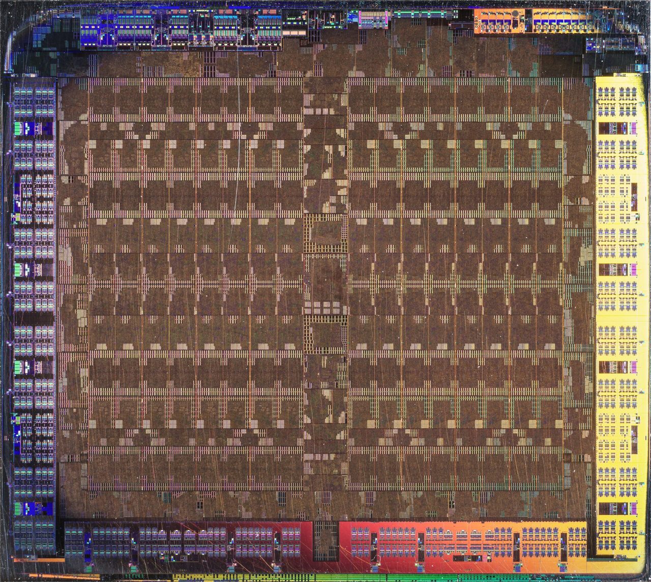
AMD's graphics come from ATI, the Canadian company it bought in 2006, and for AMD's first years with it the design was very different from Nvidia's. Tahiti replaced that design with a block called the compute unit (CU), in an architecture called Graphics Core Next (GCN), and every AMD GPU since descends from it: the chips in the PlayStation 4 and the Xbox One, the RDNA chips in today's Radeon cards and the PlayStation 5, and the CDNA chips in the Instinct accelerators that compete with Nvidia's H100 and B200 in data centres. This part opens the compute unit, follows the two directions it has been pulled in since, and puts Part 9's SM beside it at each step. Seeing a second answer to the same problem is the quickest way I know to tell which parts of a GPU are necessary and which are choices.
Side note: what GCN replaced. ATI's chips from 2007 to 2011, the TeraScale designs, were built around very wide instructions. Each lane had four or five arithmetic units, and the compiler's job was to find that many independent operations in one thread's program and pack them into a single bundle. Graphics suits this, because a colour has four parts and a position has four coordinates, and they can all be worked on at once. General computing often does not: a chain of steps that each need the last one's answer gives the compiler one operation to put in a five-wide bundle, and the other four slots go empty. GCN gave up on finding parallelism inside one thread and found it across threads instead, one simple operation per lane, which is the bet Nvidia had made with the G80 in 2006.
A phrasebook
The two companies use different words for nearly everything, which makes comparing them harder than it should be. Here is the translation the rest of this part relies on.
| Nvidia | AMD | What it is |
|---|---|---|
| streaming multiprocessor (SM) | compute unit (CU) | the repeated building block, with its own schedulers, lanes, registers and scratchpad |
| CUDA core | stream processor | one lane: a multiply-add unit working for one thread at a time |
| warp, 32 threads | wavefront or wave, 64 or 32 threads | the group of threads that shares one instruction stream |
| thread block | workgroup | threads that run together on one SM or CU and can share its scratchpad |
| shared memory | local data share (LDS) | the programmer-managed scratchpad inside the block |
| texture processing cluster (TPC) | work-group processor (WGP), on RDNA | a pair of blocks; AMD's pair shares its caches and scratchpad |
| graphics processing cluster (GPC) | shader engine | a group of blocks with its own share of the graphics front end |
| tensor core | matrix core (CDNA), AI accelerator (RDNA 3 onwards) | hardware for multiplying small matrices |
| uniform datapath (since Turing, 2018) | scalar unit | hardware for values that are the same for every thread in the group |
| L2 cache | L2 cache, then Infinity Cache | the chip-wide cache; AMD adds a large last level in front of memory |
| CUDA | HIP, part of ROCm | the programming model and software stack of Part 14 |
Two of these deserve a word now. A wavefront is exactly what a warp is, a group of threads defined by the hardware because it maps onto the lanes, but its size has been 64 for most of AMD's history and is now 32 or 64 depending on the chip. And the scalar unit has no counterpart in Part 9's drawing of the SM. It turns out to be one of the more interesting ideas in AMD's design, and it gets its own section below.
The GCN compute unit
A GCN compute unit has 64 lanes, half as many as an Ada SM, and it divides them differently. Instead of four partitions of 32 lanes, each with its own scheduler, it has four SIMDs of 16 lanes each and one scheduler for the whole unit. Each SIMD has its own 64 KB of vector registers, the per-thread registers that Part 9 called the register file, and its own ten slots for resident wavefronts. Beside the four SIMDs sits a fifth execution unit, the scalar unit, with 8 KB of registers of its own. Then come the things the whole compute unit shares: 64 KB of local data share, a 16 KB L1 cache, and the texture units that fetch and filter data from memory. One level up, each group of up to four neighbouring compute units shares an instruction cache and a cache for scalar data.
Add it up and a GCN compute unit has 64 lanes, 256 KB of vector registers, and room for 40 wavefronts of 64 threads, which is 2,560 threads, more than the 1,536 an Ada SM keeps resident. The HD 7970 has 32 compute units: 2,048 lanes, which AMD calls stream processors, and 8 MB of vector registers.
Four cycles per instruction
Here is the oddity. A wavefront has 64 threads and a SIMD has 16 lanes, so a SIMD cannot carry out one instruction for a whole wavefront at once. It does it in four goes: threads 0 to 15 on the first cycle, 16 to 31 on the second, 32 to 47 on the third, and 48 to 63 on the fourth. One instruction for one wavefront occupies its SIMD for four cycles.
That sounds like a weakness, and it is the heart of the design. The scheduler works in a matching rhythm. On each cycle it serves one of the four SIMDs, in turn, so each SIMD is handed a new instruction exactly every four cycles, exactly when it has finished the last one. Four SIMDs, each a quarter of the way further into a four-cycle job than its neighbour, keep all 64 lanes busy on every cycle, and the scheduler only has to make one decision per cycle for the whole compute unit rather than four.
The rhythm has a second payoff. Part 5's pipeline means that an arithmetic unit's answer is not ready on the very next tick. It comes out a few stages later, and an instruction that needs it has to wait. On GCN it never has to, because the next instruction for the same wavefront cannot issue for four cycles anyway, and by then the answer has emerged. One wavefront can run a chain of dependent arithmetic at full speed with no help from any other. On an SM, a warp waiting for its own last result has to be covered by a different warp. GCN's rhythm covers it by construction.
When the scheduler serves a SIMD it can do more than one thing at once. It looks at that SIMD's ten wavefronts and can issue up to five instructions in the same cycle, as long as each is a different kind and each comes from a different wavefront: one vector arithmetic instruction, one scalar instruction, one load or store to memory, one access to the local data share, and one branch. So while wavefront 3 does a multiply on the lanes, wavefront 7 can be starting a load and wavefront 1 can be counting round a loop on the scalar unit.
The cost of the rhythm is just as built in. A single wavefront can never issue more than one instruction every four cycles, so on its own it moves at a quarter of the clock rate. GCN is fast when there are many wavefronts to choose from and slow when there are few. Keep that in mind for RDNA below.
Occupancy works as it does on an SM. A SIMD's 64 KB of vector registers holds 256 registers for every thread of a wavefront if only one wavefront is resident, and the resident wavefronts divide those 256 between them. A program that needs 24 registers per thread can fill all ten slots; one that needs 128 fits only two, and with only two wavefronts to alternate between, every trip to memory shows. So the first question a profiler asks on AMD is the same as on Nvidia: how many waves are resident per SIMD?
The scalar unit
Look at what a thread actually computes and a good deal of it is not really per-thread. A loop counter is the same for all 64 threads of a wavefront. So is the address where an array starts, the size of a matrix, a constant read from memory, and the decision whether to go round the loop again. On the SM as Part 9 drew it, every one of those is worked out 32 times, once per lane, with 32 identical answers. GCN works them out once.
That is what the scalar unit is for. It runs instructions that belong to the wavefront rather than to any one thread, on the scalar registers, of which each wavefront can have about a hundred. It does integer arithmetic, loads the values every thread needs through its own small cache, and makes the branching decisions. The compiler sorts the program into the two kinds, vector instructions for values that differ from thread to thread and scalar instructions for values that do not, and the scheduler sends each to its own unit, in the same cycle if they come from different wavefronts. Every value worked out on the scalar unit is one that 64 lanes no longer have to work out 64 times. Nvidia came round to the same idea with Turing in 2018, which added a small uniform datapath with registers of its own for exactly these values.
The scalar unit is also where an if is decided, and AMD's instruction set makes visible what Nvidia's keeps inside the hardware. Every wavefront has a 64-bit execution mask, one bit per thread, held in scalar registers, and a vector instruction only changes the threads whose bit is set. This is the masking from Part 9's divergence demo, but on AMD the mask is an ordinary register that the program itself reads and writes. Here is Part 9's if (x > 0) { A } else { B } the way a GCN compute unit runs it, in GCN's assembly language, slightly simplified, with my comments:
v_cmp_lt_f32        vcc, 0, v0          ; vector: every lane tests 0 < x
s_and_saveexec_b64  s[2:3], vcc         ; scalar: save mask, keep lanes with x > 0
s_cbranch_execz     skip_A              ; scalar: no lane left? jump past A
    ...A...                             ; vector: A, on the lanes still on
skip_A:
s_andn2_b64         exec, s[2:3], exec  ; scalar: switch to the other lanes
s_cbranch_execz     skip_B              ; scalar: no lane wants B? jump past it
    ...B...                             ; vector: B, on those lanes
skip_B:
s_mov_b64           exec, s[2:3]        ; scalar: every lane back on
The instructions starting with v_ run on a SIMD's lanes, and those starting with s_ run once, on the scalar unit. Two things stand out. When the lanes disagree, both A and B still run, so divergence costs exactly what it cost in Part 9. But when they all agree, one of the s_cbranch_execz jumps skips the unwanted path entirely. That is the scalar unit earning its keep: a decision made once for the whole wavefront, on a unit that is not one of the 64 lanes, while the lanes get on with another wavefront's arithmetic.
RDNA: wave32 and the work-group processor
GCN ran Radeon cards for seven years, through chips called Hawaii, Fiji, Polaris and Vega, and it was a better compute design than a graphics one. The four-cycle rhythm needs a lot of wavefronts to keep a compute unit busy, and a game's frame is full of small jobs, and of stretches where a few long-running threads hold everything else up. In 2019 AMD redesigned the block for graphics. The new architecture, RDNA, arrived in the Radeon RX 5700 XT, on a chip called Navi 10.
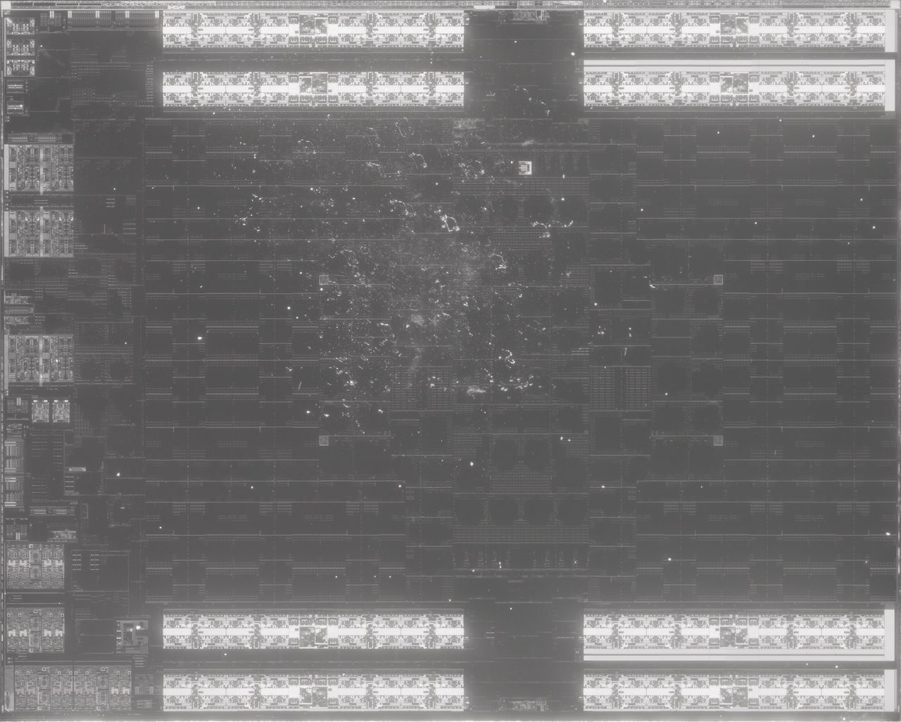
The RDNA compute unit still has 64 lanes, but as two SIMDs of 32 rather than four of 16, and its native wavefront is 32 threads, the size of an Nvidia warp. A SIMD now finishes an instruction for a whole wavefront in one cycle instead of four, and each SIMD has its own scheduler, issuing every cycle. A wavefront that used to get one instruction every four cycles can now get one every cycle, as long as its instructions do not depend on each other, and other wavefronts fill the gap when they do. The arithmetic per compute unit per cycle is unchanged, 64 lanes either way. What changed is how quickly one wavefront gets through its program, which is what matters when there are not enough wavefronts to go round.
Each SIMD also got its own scalar unit, its own 128 KB of vector registers, and twenty wavefront slots. Wave64 did not go away: an RDNA SIMD can still run a 64-thread wavefront by doing each instruction in two halves on consecutive cycles, and AMD's drivers still choose wave64 for many pixel shaders, because it halves the number of instructions the scheduler has to issue and suits work with parallelism to spare. Compute and vertex work usually runs as wave32. The compiler decides, program by program.
The other change is that compute units now come in pairs. Two of them make a work-group processor (WGP), which shares an instruction cache, a scalar data cache and a 128 KB local data share between them, so one workgroup can spread across both and use the lanes and scratchpad of two compute units. It is something like Nvidia's pairing of SMs into a TPC, but more tightly joined, because the two halves share their scratchpad.
Navi 10 has 20 work-group processors, 40 compute units in all, arranged in two shader engines with a 4 MB L2 cache behind them. The next generation, RDNA 2 in 2020, kept the block and added two things that matter later in this series: a ray accelerator in every compute unit, and a large cache in front of memory that AMD calls Infinity Cache, 128 MB of it on the biggest chip. RDNA 2 is also the graphics in the PlayStation 5 and the Xbox Series X, though without the big cache.
When the wave is wider
Why should the size of a wavefront matter so much? Partly because of the rhythm, and partly because of divergence. Part 9 showed what a warp pays when its threads disagree at an if: both paths run, with lanes switched off. The wider the group, the more likely it is to contain a disagreement somewhere. In graphics the threads are pixels, neighbouring pixels share a wavefront, and the place they disagree is wherever an edge runs through: the boundary of a shadow, the rim of a highlight, the outline of an object. Think of a wavefront of 64 as an 8 by 8 block of pixels and a wavefront of 32 as an 8 by 4 block. Real hardware packs pixels in groups of 2 by 2 and the exact shapes vary, but the effect is the same.
A patch of screen 48 pixels wide and 24 high, with a round shape in it. Every pixel runs if (inside) { A } else { B }. Drag the slider to grow the shape, and compare how the same pixels fare in waves of 64 and waves of 32. A wave whose pixels disagree, outlined in red, has to run both A and B.
wave64, as on GCN and CDNA: blocks of 8 × 8
wave32, as on RDNA, or an Nvidia warp: blocks of 8 × 4
As you drag, notice where the waste is. Deep inside the shape and well outside it, both sizes do perfectly, because every wave agrees with itself. All the waste is along the edge, and the wave64 grid wastes more there, because each wave the edge touches is twice the size and drags twice as many lanes through the path they did not need. A wave32 grid can never do worse than a wave64 one on the same pixels, since every 8 by 8 block is just two 8 by 4 blocks, and whenever the edge runs through only one of the two halves, the other half escapes. That, along with the faster rhythm, is why RDNA made 32 the native size. Nvidia has kept its warp at 32 since 2006, and it sits on the same compromise: small groups waste little at edges, big groups need fewer instructions issued for the same work.
RDNA 3 and RDNA 4
RDNA 3, in the Radeon RX 7900 XTX of December 2022, changed the compute unit again, in two ways that show up on spec sheets confusingly.
The first is dual issue. An RDNA 3 SIMD can sometimes carry out two instructions from the same wave32 in one cycle, when the compiler can find a suitable pair: two simple arithmetic operations that do not depend on each other and whose inputs sit in different banks of the register file. It can also run a wave64 arithmetic instruction in one cycle rather than two. AMD counts this in its peak figures. The RX 7900 XTX has 96 compute units, so 6,144 lanes, and a boost clock of 2.5 GHz, and with each lane doing one multiply-add, which is two operations, per cycle, that comes to
6,144 × 2 × 2.5 GHz = 30.7 TFLOPS.
AMD's figure is 61.4 TFLOPS, twice that, because it assumes every cycle is a dual-issued one. Real code gets the doubled rate only part of the time, so the honest reading of an RDNA 3 spec sheet is somewhere between the two. It is the same trap as the sparsity asterisk of Part 13: a doubling that needs the code to cooperate.
The second is matrix hardware. Each RDNA 3 compute unit has two AI accelerators, which run new matrix instructions that multiply 16 by 16 tiles across a wavefront, the same job a tensor core does, at a fraction of the rate of a data-centre chip. The high-end RDNA 3 chips also got half as much again of vector registers, 192 KB per SIMD, and one more thing, a package made of several dies, which belongs in the last section of this part.
RDNA 4, in the Radeon RX 9070 XT of March 2025, went back to a single die, called Navi 48, with 64 compute units.
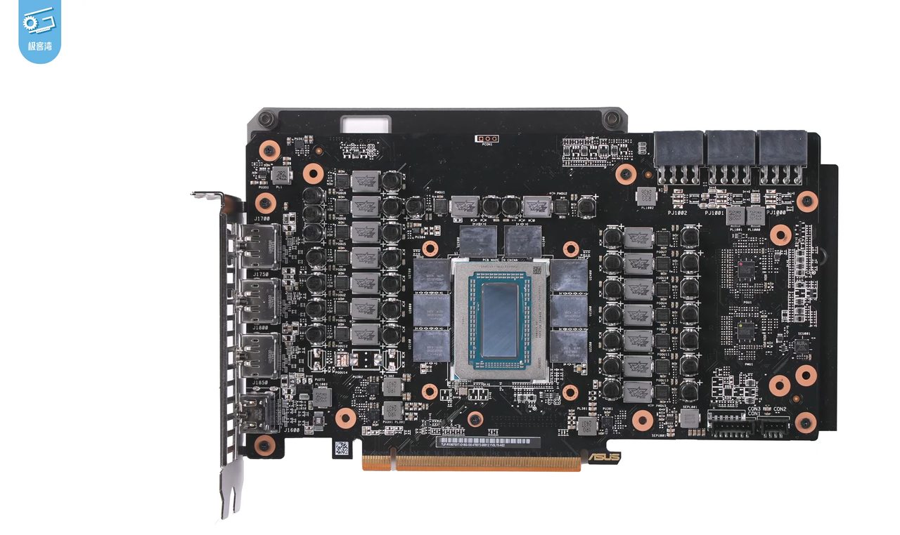
Its compute unit's most interesting change is a small one with a large idea behind it. A wavefront can now ask for more vector registers in the middle of running, and hand them back when it no longer needs them. Part 9 explained that occupancy is set by the greediest moment of a program, because registers are allocated for the whole run, so a shader that needs a hundred registers for ten instructions holds a hundred for all of them. Dynamic allocation lets it hold them only for the stretch that needs them, and the slots it frees can hold more wavefronts. Ray tracing, where some stretches of a shader need far more registers than the rest, is the case AMD had in mind. RDNA 4 also gave the AI accelerators much higher matrix rates and the FP8 format, aimed at the machine-learning upscaling that games now run on them.
CDNA: the compute line kept wave64
While RDNA went one way, AMD's data-centre chips went the other. In 2020 AMD split its GPUs into two families: RDNA for graphics, and CDNA for computing, starting with the Instinct MI100. CDNA kept GCN's compute unit almost exactly: four SIMDs of 16 lanes, wavefronts of 64, the four-cycle rhythm, the scalar unit. Supercomputer and AI code has parallelism to spare, so the rhythm's weakness, slow single wavefronts, hardly matters, and keeping the old unit kept a decade of compiler work and tuned software. What CDNA dropped was the graphics hardware of Part 20: the rasterisers, the units that write finished pixels, and the display outputs, the same choice Nvidia made when GH100 left out the RT cores.
What CDNA added was matrix hardware. Its matrix cores sit beside the SIMDs and run matrix multiply-add instructions across a whole wavefront, AMD's version of the tensor core of Part 13. Their results build up in a second set of registers, the accumulation registers, which is why a CDNA 3 compute unit has 512 KB of register space, twice a GCN unit's. The MI250X of 2021, which put two CDNA 2 dies in one package, is the chip in Frontier at Oak Ridge, the first supercomputer to pass an exaflop.
In CDNA 3, the generation in the Instinct MI300X of December 2023, each compute unit has four SIMDs and four matrix cores, a 64 KB local data share and a 32 KB L1 cache. Per clock, one compute unit does 256 FP32 operations on its ordinary lanes, 2,048 FP16 operations on its matrix cores, and 4,096 at FP8. Set that beside Part 9's SM. One Hopper SM's tensor cores do about 4,096 dense FP16 operations per clock, twice a CDNA 3 compute unit. The MI300X answers with numbers: 304 compute units against the H100's 132, which at 2.1 GHz comes to
304 × 2,048 × 2.1 GHz = 1,307 TFLOPS of dense FP16,
against the H100's 989. It is a trade that recurs all through this series: a smaller block, and more copies of it.
The split did not last for ever. CDNA 5, the generation in the MI455X of 2026, gave up the four SIMDs of 16 and the four-cycle rhythm, and builds its compute dies from RDNA-style work-group processors running wave32, four SIMDs of 32 lanes to each. After six years apart, the data-centre block came round to the graphics one. Part 30 has the details.
From compute unit to package
The levels above the compute unit follow Nvidia's plan. Compute units, in pairs on RDNA, are grouped into shader engines, AMD's equivalent of a GPC, each with its own share of the graphics front end, and behind them sits an L2 cache shared by the whole chip and, on recent chips, an Infinity Cache behind that. Navi 10 has two shader engines of ten WGPs; Navi 31, the chip in the RX 7900 XTX, has six of eight.
Where AMD parts company with Nvidia is in how it builds the biggest chips. Part 3 showed why no die can grow past the reticle limit, and Part 19 why big dies yield badly. Nvidia's answer, in Part 27's Blackwell, is two dies at the reticle limit joined edge to edge. AMD's answer, since 2022 for graphics and 2023 for data centres, has been to cut the GPU into chiplets: several smaller dies, each made on whatever process suits its job, packaged together so that they behave as one GPU.
Navi 31 is one graphics compute die of about 300 mm² holding all 96 compute units, made on TSMC's 5 nm process, with six memory cache dies of about 37 mm² made on the cheaper 6 nm. Each memory cache die holds 16 MB of Infinity Cache and a 64-bit slice of the memory interface. The circuits that drive signals off the chip to the memory, and to a lesser degree cache memory, barely shrink on a newer process, so there was little point in paying 5 nm prices for them.
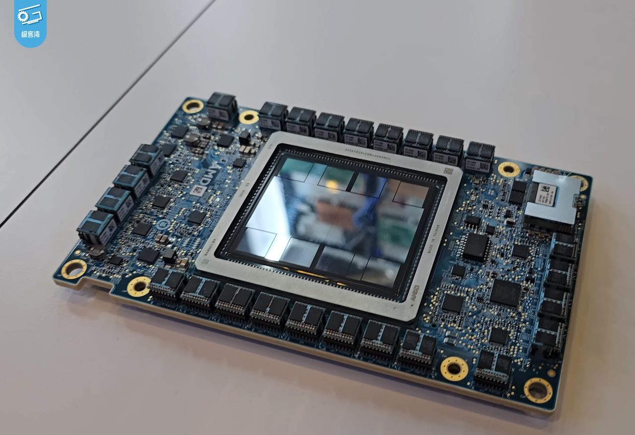
The MI300X goes much further. Eight accelerator complex dies (XCDs), each with 38 working compute units of 40 and a 4 MB L2 cache, are bonded directly on top of four I/O dies, copper to copper, two XCDs to each. The I/O dies hold 256 MB of Infinity Cache between them, the controllers for eight stacks of HBM3, and the links to other GPUs, and the whole assembly sits on one silicon interposer beside the memory, the CoWoS construction of Part 19. Twelve pieces of logic silicon and eight stacks of memory, 153 billion transistors, presented to software as one GPU with 192 GB. A close relative, the MI300A, swaps two of the XCDs for three CPU chiplets with 24 Zen 4 cores between them, and is the chip in El Capitan at Lawrence Livermore.
And here is the real thing, or its successor, which is the same package with more memory.
Here are the four chips of this part side by side.
| Radeon HD 7970 | Radeon RX 5700 XT | Radeon RX 7900 XTX | Instinct MI300X | |
|---|---|---|---|---|
| Chip, architecture, year | Tahiti, GCN, 2012 | Navi 10, RDNA, 2019 | Navi 31, RDNA 3, 2022 | 8 XCDs on 4 I/O dies, CDNA 3, 2023 |
| Process | TSMC 28 nm | TSMC 7 nm | TSMC 5 nm and 6 nm | TSMC 5 nm and 6 nm |
| Transistors | 4.3 billion | 10.3 billion | about 58 billion, 7 dies | 153 billion, 12 dies |
| Compute units | 32 | 40, in 20 WGPs | 96, in 48 WGPs | 304, of 320 built |
| Stream processors (lanes) | 2,048 | 2,560 | 6,144 | 19,456 |
| Wavefront | 64 | 32 or 64 | 32 or 64 | 64 |
| Vector registers per CU | 256 KB | 256 KB | 384 KB | 512 KB, with accumulation registers |
| Local data share | 64 KB per CU | 128 KB per WGP | 128 KB per WGP | 64 KB per CU |
| Caches | 768 KB L2 | 4 MB L2 | 6 MB L2, 96 MB Infinity Cache | 32 MB L2, 256 MB Infinity Cache |
| Memory | 3 GB GDDR5, 264 GB/s | 8 GB GDDR6, 448 GB/s | 24 GB GDDR6, 960 GB/s | 192 GB HBM3, 5.3 TB/s |
| FP32 peak | 3.8 TFLOPS | 9.75 TFLOPS | 61.4 TFLOPS, with dual issue | 163.4 TFLOPS |
| Board power | 250 W | 225 W | 355 W | 750 W |
Read down the columns and the shape of the decade is there. The compute unit stayed recognisably the same block, 64 lanes with a scalar unit beside them, while the graphics line made it nimbler and the data-centre line made it bigger and bolted matrix cores on. The memory bandwidth grew twentyfold, and the number of compute units nearly tenfold, but the biggest change is in the transistor row: one die became seven, then twelve.
Where this leaves us
AMD's compute unit and Nvidia's SM are two answers to one problem, and the answers agree more than they differ. Both put a few dozen to a few hundred copies of one block on a chip. Both keep many groups of threads resident and switch between them for free, both pay for disagreement at an if by running both paths with lanes switched off, and both now attach matrix hardware to the lanes. The differences are the instructive part: a wavefront of 64 and a four-cycle rhythm that hides the pipeline by construction, a scalar unit that does once-per-wavefront work once, compute units in pairs that share their scratchpad, and a habit of building the biggest GPUs out of chiplets. And AMD now has two blocks rather than one: RDNA's, tuned for the short, branchy work of a game frame, and CDNA's, which kept the old rhythm because supercomputers and AI training have parallelism to spare, until in 2026 it too moved to wave32.
There is a third company with a block of its own design, and its answers to the same questions differ again: a group width that the compiler chooses for each program, a register file with a fixed seat for every thread, and memory reached by sending messages. That is the next part. After it, Part 12 takes up the problem all three blocks share: keeping thousands of lanes fed from a memory that cannot keep up.
Next: Inside an Intel Xe-core: Intel's building block, vector engines and matrix engines, hardware threads whose width the compiler chooses, a register file with a fixed seat for every thread, and how Battlemage rebuilt the core with half as many engines twice as wide.