Part 9 opened Nvidia's building block and Part 10 AMD's. There is a third company with a GPU of its own design, and by one count it is the largest of the three. Intel has put graphics into most of the PC processors it has sold since 2011, so for years more computers have drawn their screens with an Intel GPU than with anyone else's. What Intel did not have, until 2022, was a graphics card worth buying, and the block it built to make one is called the Xe-core.
The Xe-core answers the same questions as the SM and the compute unit, how many lanes per instruction, how many threads waiting, what to do at an if, and it answers two of them differently enough to be worth a part of its own. The width of a group of threads is not fixed by the hardware but chosen by the compiler, program by program. And the register file gives every thread a fixed seat, rather than dividing itself among however many threads fit. Both choices come from Intel's long history with integrated graphics, and both are easiest to see by putting the Xe-core beside the two blocks you already know.
A three-way phrasebook
Part 10 needed a phrasebook for two companies. Intel brings a third set of names, and some of them collide with the other two in confusing ways, so here is the table again with a column added.
| Nvidia | AMD | Intel | What it is |
|---|---|---|---|
| streaming multiprocessor (SM) | compute unit (CU) | Xe-core | the repeated building block |
| SM partition, with its scheduler | SIMD | Xe Vector Engine (XVE), once called an execution unit (EU) | the slice of the block that issues instructions to a set of lanes |
| CUDA core | stream processor | (no product name; a lane of an XVE) | one lane: a multiply-add unit |
| warp, 32 threads | wavefront, 64 or 32 | hardware thread, 8, 16 or 32 work-items wide; a sub-group in the code | the group that shares one instruction stream |
| thread | thread or work-item | work-item | one instance of the program, one lane's worth of work |
| thread block | workgroup | work-group | threads that share the block's scratchpad |
| shared memory | local data share (LDS) | shared local memory (SLM) | the programmer-managed scratchpad |
| graphics processing cluster (GPC) | shader engine | render slice | a group of blocks with its share of the graphics hardware |
| tensor core | matrix core | Xe Matrix eXtensions (XMX) engine | hardware for small matrix multiplies |
| CUDA | HIP, ROCm | SYCL, oneAPI, Level Zero | the programming model and software stack |
The collision to watch is the word thread. To Nvidia a thread is one lane's worth of work, and 32 of them make a warp. To Intel's hardware a thread is the whole group: one instruction stream, one program counter, issuing each instruction across 8, 16 or 32 lanes' worth of data at once. The individual lanes' worth of work are work-items. So an Intel hardware thread is, near enough, a warp, and the rest of this part uses the word in Intel's sense, with "hardware thread" where there could be doubt.
The Alchemist Xe-core
Intel's first discrete graphics architecture of the modern era, Xe-HPG, shipped in the Arc A-series cards of 2022 under the code name Alchemist. Its Xe-core has 128 lanes, the same as an Ada SM, but it slices them much more finely. There are sixteen vector engines of eight lanes each, every one with its own share of the register file and room for eight hardware threads, and pairs of them share a thread-control unit that picks what to issue. Beside them sit sixteen XMX matrix engines, Intel's tensor cores, one per vector engine. Shared across the whole core are 192 KB of memory that serves as both L1 cache and shared local memory, a texture sampler, a load-store unit, and a ray-tracing unit.
Add up an Alchemist Xe-core: 128 lanes, which do 256 FP32 operations per clock as multiply-adds, 512 KB of registers, 128 hardware threads, and XMX engines that together do 2,048 FP16 or 4,096 eight-bit integer operations per clock. The Arc A770 has 32 of these cores, 4,096 lanes in all, and at its 2.1 GHz that is 17.2 TFLOPS of FP32 and about 138 TFLOPS of FP16 matrix arithmetic.
Notice the register file. An Ada SM has 256 KB for 128 lanes, a GCN compute unit 256 KB for 64. The Xe-core has 512 KB for 128 lanes, twice the SM's, and the reason is the next two sections.
Threads whose width the compiler chooses
On an Nvidia GPU the group is always 32. On AMD's it is 64, or 32 on RDNA when the compiler asks for it. On Intel's the compiler picks a width for every program it compiles, and Alchemist accepts three: eight, sixteen or thirty-two work-items per hardware thread, called SIMD8, SIMD16 and SIMD32. A vector engine has eight lanes, so a SIMD8 thread finishes an instruction in one pass, a SIMD16 thread takes two, and a SIMD32 thread four, much as GCN's sixteen lanes took four passes over a wavefront of 64.
Why let the width vary? Because the right width depends on the program, and the compiler can see the program. A wider thread covers more work-items per instruction issued, which is efficient when the code is simple and every work-item agrees. A narrower thread wastes less when the work-items disagree at an if, the lesson of the divergence demo in Part 9 and the wave32 demo in Part 10, and, as the next section shows, leaves more registers for each work-item. Intel's graphics compilers have made this choice for each shader since the company's integrated GPUs of the late 2000s. In code, the width shows up as the sub-group size of SYCL, Intel's equivalent of the warp size, which a programmer can request or leave to the compiler.
Eight hardware threads per vector engine is fewer than it sounds like next to an SM partition's twelve warps, but there are sixteen vector engines, so an Alchemist Xe-core holds 128 hardware threads, and at SIMD16 that is 2,048 work-items resident, more than an Ada SM's 1,536. The thread-control unit does what Part 9's warp scheduler does: each cycle, find a thread whose next instruction is ready and issue it, so that a thread waiting 400 cycles for memory costs nothing while the others run.
A fixed seat for every thread
Here is the bigger difference. On an SM, Part 9 explained, the register file is divided among the resident warps according to need: a program that uses 42 registers per thread fits 48 warps, one that uses 100 fits far fewer, and occupancy falls as register use rises. The compute units of Part 10 work the same way. An Intel vector engine does not. It always has its eight threads, and each always gets the same slice of the register file: 128 registers, which on Alchemist are 32 bytes wide, 4 KB per thread. On Battlemage they are 64 bytes wide, 8 KB per thread.
What a thread does with its 128 registers depends on its width. A 32-byte register holds eight 32-bit numbers, so for a SIMD8 thread one register is one variable for every work-item, and the thread can keep 128 variables per work-item. For a SIMD16 thread each variable takes two registers, so 64 variables; for SIMD32, four registers and 32 variables. If a program needs more than its seat holds, the compiler has two choices. It can compile for a narrower width, giving each work-item more room, or it can spill: store some values in memory and fetch them back when needed, which is slow. There is also a large register file mode, 256 registers per thread with only four threads per vector engine, first on Intel's data-centre GPUs and, through driver updates, on its Arc graphics too. It is the SM's trade, fewer threads for more registers each, offered as a single switch rather than a sliding scale.
Try it below. Pick an architecture, a width and the number of 32-bit values each work-item needs, and compare what fits with what an Ada SM would do with the same program.
One program, two kinds of register file. Choose how many 32-bit values each work-item keeps in registers, the Intel architecture, the SIMD width, and the register mode.
Drag the slider up and watch the two bars behave differently. The SM's bar falls in steps from the start, because every extra register per thread is taken from the pool the other warps share. The Xe-core's bar stays flat, the same 2,048 work-items whatever the program uses, and then drops off a cliff: past the seat's size the program no longer fits at that width, and the compiler has to spill, narrow the width, or trade half the threads for the large mode. Neither design is better in general. The fixed seat makes the hardware simpler and the occupancy predictable, and it is one reason the Xe-core needs a larger register file than the SM, since every seat is sized for a demanding program whether or not the running program is one.
Intel has since moved towards the SM's way. The next generation, Xe3, in the Panther Lake laptop processors of 2026, hands out registers in blocks of 32 according to need: a vector engine runs ten threads when each needs 96 registers or fewer, and fewer threads as needs grow, so that occupancy, in the words of the Chips and Cheese analysis of Xe3, degrades more gracefully. Three companies, and the register file has converged on one idea.
Messages instead of loads
There is no separate scalar unit in an Xe-core, of the kind Part 10 described in AMD's compute unit. A vector engine can run an instruction on a single lane, written SIMD1, which serves for loop counters and addresses, so the work AMD sends to a scalar unit runs on the same lanes at a width of one. Intel's notable difference is elsewhere, in how a thread reaches anything outside its own registers.
A vector engine's instructions cover arithmetic on registers and nothing else. Every load, every store, every texture read, every access to shared local memory, is done by a send instruction, which packages a request as a message and posts it to a unit shared by the whole Xe-core: the load-store unit for memory, the sampler for textures, a separate unit for shared local memory. The answer comes back into the sending thread's registers some time later, and the thread-control unit knows not to issue anything that needs it until it arrives. It is the same latency-hiding of Part 9, with the waiting expressed as a message in flight rather than a load in a pipeline, and it is a design inherited directly from Intel's integrated GPUs, where the shared units were also shared with the rest of the processor.
Battlemage: half as many engines, twice as wide
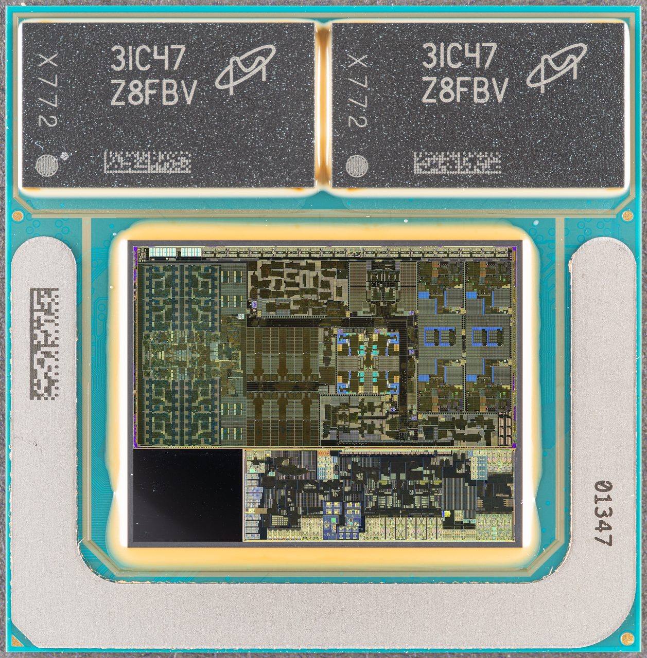
The second generation, Xe2, appeared in the Lunar Lake laptop processors of September 2024 and in the Arc B580 graphics card that December, under the code name Battlemage. Its Xe-core keeps the totals and changes the slicing. The sixteen vector engines of eight lanes became eight of sixteen, and the sixteen matrix engines became eight of twice the width. The core still has 128 lanes, 512 KB of registers and the same matrix throughput per clock, but each vector engine now runs SIMD16 in a single pass and SIMD32 in two, and the narrowest width, SIMD8, was dropped. The shared L1 and local memory grew from 192 to 256 KB.
Why halve the number of engines? Each vector engine needs its own instruction issue, its own thread bookkeeping and its own share of wiring, and those costs are much the same whether the engine has eight lanes or sixteen. Fewer, wider engines spend less silicon and power per lane on control, which is the argument of Part 6 made one level down. The cost is the familiar one, that a wider group wastes more when its work-items disagree. Intel judged that most real shaders already ran at SIMD16 or wider, and claimed about 70 per cent more performance per Xe-core than Alchemist, much of it from keeping the wider engines busier and from higher clocks. Each engine also gained a cleaner split between its two arithmetic units, one for floating point and one for integer work, so that the address arithmetic every shader does can run beside its floating-point maths.
XMX: the matrix engines
The XMX engines work much as Part 13 will describe for tensor cores. A single instruction, called DPAS for dot product accumulate systolic, takes small tiles of two matrices from a hardware thread's registers and adds their product into a third, working through them in a systolic array, the grid of multiply-add cells through which numbers flow from one cell to the next, which Part 32 explains in the context of NPUs and Google's TPU. On Alchemist and Battlemage alike an Xe-core's engines do 2,048 FP16 or BF16 operations per clock and 4,096 at 8-bit integer precision. The data-centre version of the core, Xe-HPC, in the Ponte Vecchio chip of Part 26, has engines twice as large again, 4,096 FP16 operations per core per clock. And the Xe3P core of 2026, in Intel's Crescent Island inference chip, made its matrix engines about four times larger than Battlemage's and added FP8 and FP4.
Intel uses the matrix engines on its gaming cards for the same purpose as Nvidia and AMD do on theirs: XeSS, a neural-network upscaler that renders each frame at a lower resolution and fills in the rest, and since 2024 generates whole frames as well. Part 23 has more on that.
From Xe-core to die
Above the Xe-core the plan is familiar. Four Xe-cores, with four ray-tracing units and the fixed-function graphics hardware of Part 20, make a render slice, Intel's equivalent of a GPC or a shader engine. The render slices share an L2 cache and the memory controllers. The flagship Alchemist chip, ACM-G10 in the Arc A770, has eight render slices; the Battlemage chip in the Arc B580, BMG-G21, has five.
Here are the blocks of the three companies side by side, one generation each, per block.
| Ada SM (Nvidia, 2022) | RDNA compute unit (AMD, 2019) | Alchemist Xe-core (Intel, 2022) | Battlemage Xe-core (Intel, 2024) | |
|---|---|---|---|---|
| Lanes | 128 | 64 | 128 | 128 |
| Issuing units | 4 partitions of 32 lanes | 2 SIMDs of 32 lanes | 16 vector engines of 8 lanes | 8 vector engines of 16 lanes |
| Group width | 32, fixed | 32 or 64 | 8, 16 or 32, chosen by the compiler | 16 or 32 |
| Groups resident | 48 warps | 40 wavefronts | 128 hardware threads | 64 hardware threads |
| How registers are shared | divided by need | divided by need | a fixed 4 KB seat per thread | a fixed 8 KB seat per thread |
| Register file | 256 KB | 256 KB | 512 KB | 512 KB |
| Scratchpad and L1 | 128 KB, shared | 128 KB per pair, plus L0 | 192 KB, shared | 256 KB, shared |
| Values worked out once per group | uniform datapath | scalar unit | SIMD1 on the same lanes | SIMD1 on the same lanes |
| Matrix hardware | 4 tensor cores | none | 16 XMX engines | 8 XMX engines, twice as wide |
Where this leaves us
Three companies, three blocks, one design. Every one of them is a few dozen to a few hundred copies of a unit with something over a hundred lanes, a big register file, a pool of resident thread groups to switch between while memory answers, a scratchpad for tiles, and matrix hardware bolted beside the lanes. The Xe-core's particular choices come from Intel's integrated graphics: a group width the compiler chooses per program, a register file with a fixed seat for each of a fixed number of threads, at least until Xe3, and a vector engine that reaches everything beyond its registers by sending messages to shared units. Battlemage then traded sixteen narrow engines for eight wide ones, the same direction of travel as everyone else's, towards less control per lane.
What none of the three blocks can do on its own is keep itself fed. Each lane does a multiply-add every tick, and every one of those needs two numbers in and one out. Across a whole chip that is tens of trillions of numbers a second, and the memory of Part 7 delivers nowhere near that. How the gap gets closed is the next part, and it is where the design of a GPU becomes a design of its memory.
Next: Feeding the Cores: the GPU memory hierarchy from registers to HBM, the roofline that tells you whether your job is starved of arithmetic or of bytes, and why a language model generating text is almost always the second.