Part 21 took apart Nvidia's gaming chip. AMD's gaming chips of the same years were built for the same job on a smaller budget, and the interesting thing about them is where the budget went. Three generations of RDNA, AMD's graphics design since 2019, ran from late 2020 to 2025. Each one tried a different answer to the question Ada answered with a 72 MB cache: how do you feed a fast graphics chip when the memory chips on the board have stopped getting faster? This part follows those answers, and then follows the same design out of the PC into the consoles and handhelds, where most RDNA chips actually live.
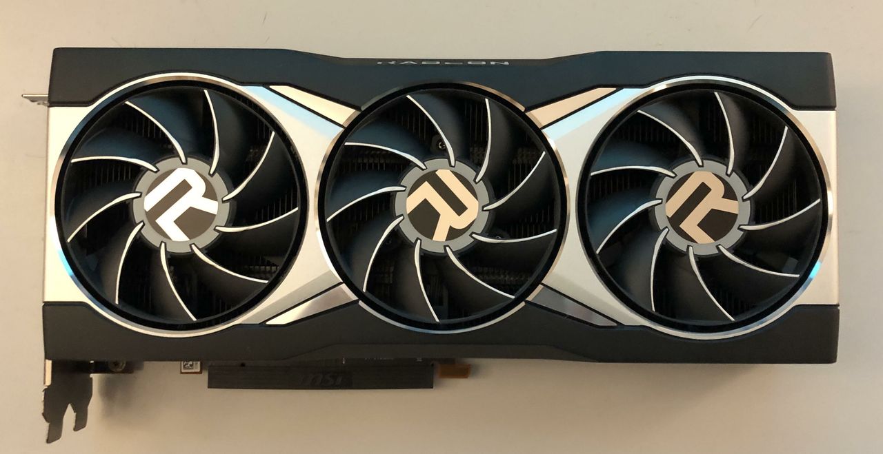
By the numbers
| RX 6900 XT (RDNA 2) | RX 7900 XTX (RDNA 3) | RX 9070 XT (RDNA 4) | RTX 4090 (Ada), for comparison | |
|---|---|---|---|---|
| Launched | December 2020, $999 | December 2022, $999 | March 2025, $599 | October 2022, $1,599 |
| Chip | Navi 21, one die | Navi 31, seven dies | Navi 48, one die | AD102, one die |
| Transistors, area | 26.8 billion, 520 mm² | about 58 billion, 300 mm² plus 6 × 37 mm² | 53.9 billion, 357 mm² | 76.3 billion, 608 mm² |
| Process | TSMC 7 nm | TSMC 5 nm and 6 nm | TSMC 4 nm | TSMC 4N |
| Compute units or SMs | 80 CUs | 96 CUs | 64 CUs | 128 SMs |
| Lanes | 5,120 | 6,144 | 4,096 | 16,384 |
| Last-level cache | 128 MB Infinity Cache | 96 MB Infinity Cache | 64 MB Infinity Cache | 72 MB L2 |
| Memory | 16 GB GDDR6, 256-bit, 512 GB/s | 24 GB GDDR6, 384-bit, 960 GB/s | 16 GB GDDR6, 256-bit, 640 GB/s | 24 GB GDDR6X, 384-bit, 1,008 GB/s |
| FP32 peak | 23 TFLOPS | 61 TFLOPS, with dual issue | 49 TFLOPS, with dual issue | 83 TFLOPS |
| Board power | 300 W | 355 W | 304 W | 450 W |
Two things in the table are worth noticing before going further. The memory buses are narrow: two of the three Radeons have a 256-bit bus where the Nvidia card has 384. And the most recent Radeon is not the biggest. The RX 9070 XT has fewer compute units than the RX 7900 XTX it followed, on one die rather than seven, at a much lower price. Both are deliberate, and each has a section below.
The cache that does the bus's job
When AMD designed Navi 21 it faced the problem Part 21 described for Ada, two years earlier. GDDR6 on a circuit board had run into the limits of Part 12: faster signalling costs power, and a wider bus needs more memory chips, more wires through the board, and a bigger, hotter interface on the die. Nvidia's RTX 3090 of the same year used a 384-bit bus of the faster, hotter GDDR6X to reach 936 GB/s. AMD's engineers estimated that to feed 80 compute units the conventional way they would have needed a 512-bit bus, with all the power, area and cost that goes with it.
They built a cache instead. Infinity Cache is 128 MB of on-die memory sitting between the chip's ordinary 4 MB L2 cache and the GDDR6, and every read that goes out to memory passes through it first. AMD's engineers said they borrowed the idea from the large L3 caches of their EPYC server processors. A game frame reads the same textures, geometry and intermediate images many times over, so if the cache holds most of what the frame is working on, most reads never leave the chip. AMD's figure was an average hit rate of 58 per cent across popular games at 4K, and higher at lower resolutions, where a frame's working set is smaller.
What does a 58 per cent hit rate buy? If 58 of every 100 reads are answered on the chip, only 42 reach the memory bus, so the bus can sustain traffic about 2.4 times its own bandwidth before it becomes the bottleneck. A 256-bit bus behaves like one roughly 610 bits wide, which is AMD's 512-bit bus and then some, at a fraction of the power, since a read from on-die SRAM costs far less energy than one that crosses the board. Try it below.
Navi 21 with its 256-bit GDDR6 bus at 512 GB/s and 128 MB of Infinity Cache. Drag the slider to change the share of memory reads the cache answers, and see how much traffic the compute units can sustain before the bus or the cache runs out.
AMD's own headline for this, "up to 1,664 GB/s", is the cache's bandwidth weighted by the hit rate plus the bus's, which is a slightly different sum from the one in the demo. Both say the same thing: the cache roughly doubles or triples what the narrow bus can do, and it does so more as the hit rate climbs. The catch is the hit rate itself. At 4K, two in five reads still go out to memory, and the numbers fall away faster than the cache can grow. Doubling the cache from 64 to 128 MB helped a lot at 4K and very little at 1080p, which is why AMD's cheaper chips got smaller caches matched to the resolutions they were meant for, 96 MB on Navi 22, 32 MB on Navi 23.
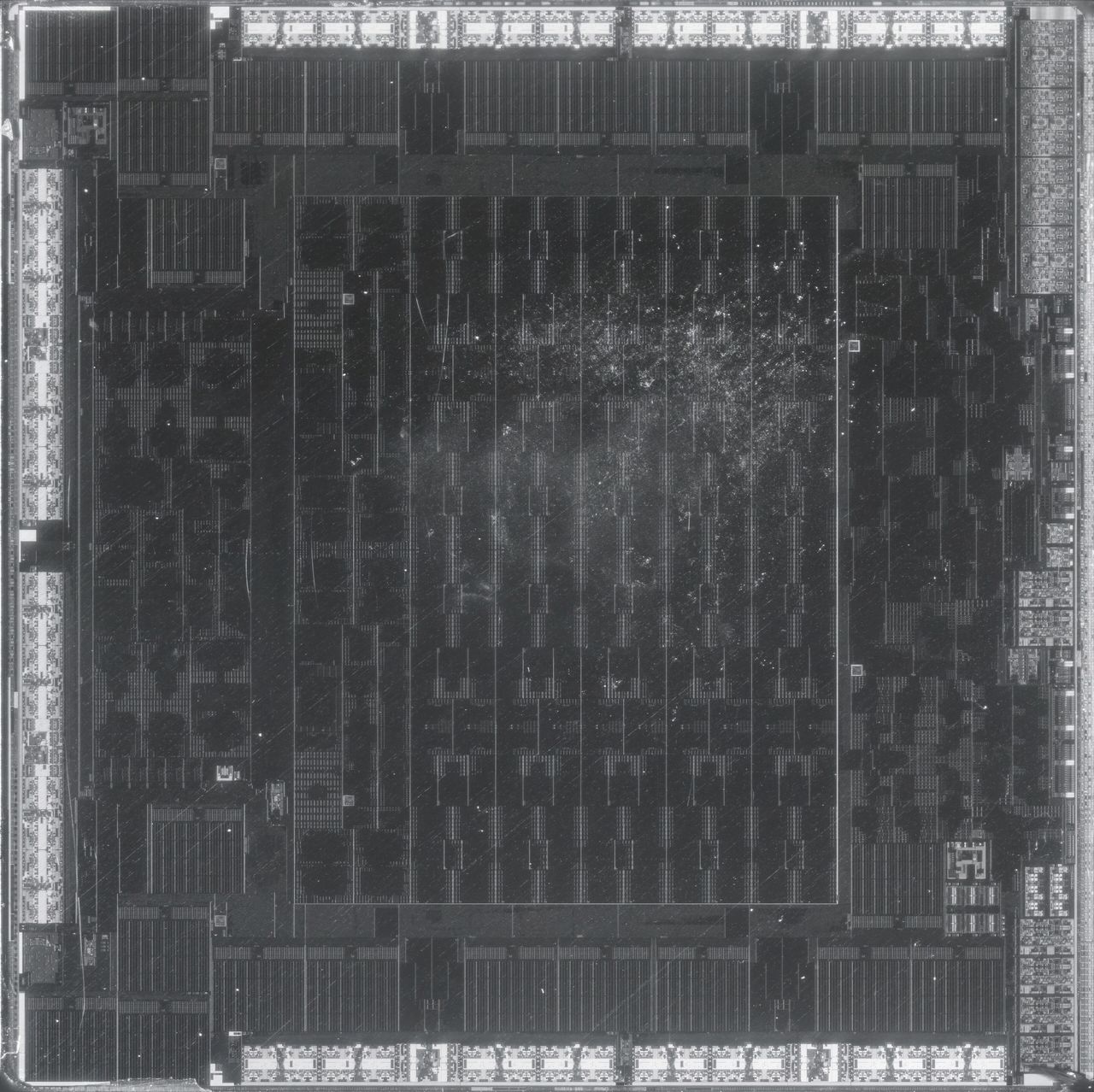
Two years later Nvidia did the same thing in its own way. Ada's L2 grew from 6 MB to 96 MB for exactly the reason Navi 21's cache existed, and Part 21 calls it the single biggest change in that generation. The two companies arrived at large on-die caches from different directions, AMD from its server processors and Nvidia from its data-centre GPUs, and both arrived because GDDR on a board had stopped keeping up with the arithmetic.
Ray tracing, half in hardware
RDNA 2 was also AMD's first design with hardware for ray tracing, and it is worth comparing with Nvidia's, because they put the line between hardware and software in different places. Part 21 explained the job: a ray descends a bounding volume hierarchy, a tree of nested boxes, testing itself against boxes until it reaches a few triangles to test exactly. There are two kinds of work in that. One is the tests themselves, which are fixed arithmetic. The other is walking the tree: deciding which box to open next, remembering the ones still to visit, and fetching the next node from memory.
Nvidia's RT cores do both in hardware. A shader hands the RT core a ray and gets back a hit. AMD's ray accelerators, one per compute unit, built into the texture unit, do only the tests, four box tests or one triangle test per clock. The walking is done by ordinary shader code running on the compute unit's lanes, with the list of boxes still to visit kept in the local data share. That saved silicon, and it cost in exactly the place Part 9 would predict. Tree walking is branchy, data-dependent code, and 32 rays in a wavefront walk 32 different paths, so the lanes spend much of their time masked off, and the registers and local memory the walk needs reduce how many other wavefronts can be resident. In games with heavy ray tracing, RDNA 2 and RDNA 3 fell well behind their Nvidia rivals.
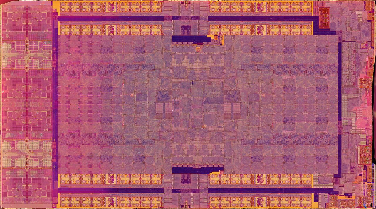
RDNA 4 is where AMD went after the gap, without moving the walk into hardware. Each ray accelerator got a second intersection engine, doubling the rate to eight box tests or two triangle tests per clock. Each node of the tree now holds eight boxes rather than four, so the tree is shallower and a ray takes fewer of the slow, memory-bound steps down it. Boxes can now be rotated to fit the object inside them, a trick called oriented bounding boxes, so a ray misses a long thin object's box more often instead of entering it for nothing. And a block of hardware now handles the step between one object's tree and the scene's, a transform that RDNA 2 did in shader code. AMD claims about twice the ray-tracing throughput per compute unit of RDNA 3. In one synthetic test measured by Chips and Cheese, a mid-range RX 9070 performed about three times as many box tests per second as the older flagship RX 6900 XT.
The chiplet gaming GPU, and the step back
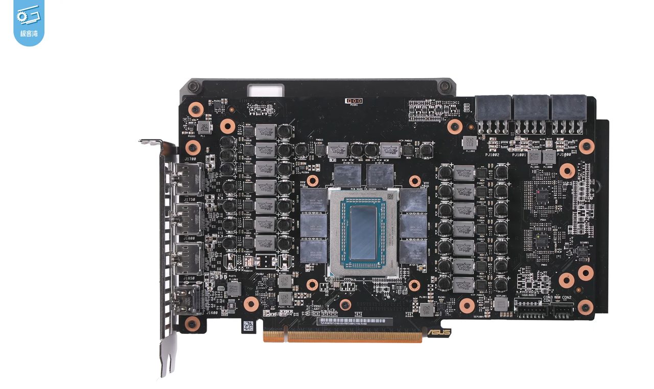
Part 10 drew Navi 31, the chip in the RX 7900 XTX: one 5 nm compute die with all 96 compute units, and six small 6 nm dies each holding 16 MB of Infinity Cache and a 64-bit slice of the memory bus, joined by wiring in the package that carries 5.3 TB/s. It was the first gaming GPU built from chiplets, and it moved the Infinity Cache off the expensive die entirely, which is the logic of the design: cache and memory interfaces barely shrink on newer processes, so they went on cheaper ones. It also ran different parts of the chip at different speeds, the front end that hands out work at 2.5 GHz and the compute units at a slightly lower 2.3 GHz, which AMD said cut the arithmetic's power by about a quarter.
It was not a 4090 rival, and AMD said so at the launch: it priced the card at $999 against Nvidia's $1,199 RTX 4080 and said that was the comparison it intended. The smaller Navi 32 also used chiplets. The smallest, Navi 33, did not.
Then RDNA 4 went back to one die. Navi 48 is 357 mm² on TSMC's 4 nm process with 64 compute units, and there is no larger RDNA 4 chip. The reason AMD gave was not technical. In September 2024 Jack Huynh, who runs AMD's computing and graphics business, said that its priority was to build scale, to get to 40 to 50 per cent of the market, so that game developers would optimise for Radeon first, and that chasing the top of the range would come later. The engineering fits that choice. Chiplets pay for themselves when a design would otherwise be a very large die on an expensive process, which a mid-range chip of 357 mm² is not, and they cost power and latency in the links between the pieces. The RX 9070 XT launched at $599, and AMD's share of desktop graphics cards still stood at around 5 to 8 per cent through 2025 and into 2026, by Jon Peddie Research's count.
Matrix units for the pictures
Nvidia put tensor cores on gaming cards in 2018 and used them for DLSS, the neural upscaler Part 21 described. AMD's answer, FidelityFX Super Resolution, was for its first three versions an ordinary hand-written algorithm that ran on any card, Nvidia's included. That was partly principle and partly necessity, since until RDNA 3 Radeons had no matrix hardware worth the name.
RDNA 3's AI accelerators, two per compute unit, did 512 FP16 operations per compute unit per clock. RDNA 4 doubled that to 1,024 and added FP8 at 2,048, which is how the RX 9070 XT reaches about 195 TFLOPS of dense FP16 and about 390 of dense FP8. That is somewhat over half of an RTX 4090's FP8 rate, on a card that cost little more than a third as much. AMD used it for FSR 4, its first upscaler built on a neural network, launched with RDNA 4 in March 2025 and, at first, for RDNA 4 only. A package AMD called Redstone followed in December 2025 with neural frame generation and a network that cleans up ray-traced lighting, the same list of jobs DLSS had taken on over the previous seven years. In June 2026 AMD brought FSR 4 to the older RX 7000 cards, with a model reworked to use the 8-bit integer arithmetic RDNA 3 does have, at a small cost in speed, and it has promised RX 6000 support in 2027.
The same chips under the television
Most RDNA chips are not on graphics cards at all. The PlayStation 5 and the Xbox Series X and S, launched in November 2020, each have a single AMD chip holding eight Zen 2 processor cores and an RDNA 2 GPU, sharing one pool of GDDR6 memory, the arrangement Part 32 calls a system on a chip. The PS5's GPU has 36 compute units running at up to 2.23 GHz, 10.3 TFLOPS, reading 448 GB/s. The Xbox Series X has 52 compute units at 1.825 GHz, 12.2 TFLOPS and 560 GB/s. The PS5 Pro of 2024 has 60 compute units in a design Sony's lead architect Mark Cerny calls RDNA 2.x, with ray-tracing hardware borrowed from what became RDNA 4 and extra matrix arithmetic for Sony's own neural upscaler. And Valve's Steam Deck runs on an AMD chip with just eight RDNA 2 compute units, 1.6 TFLOPS from a few watts.
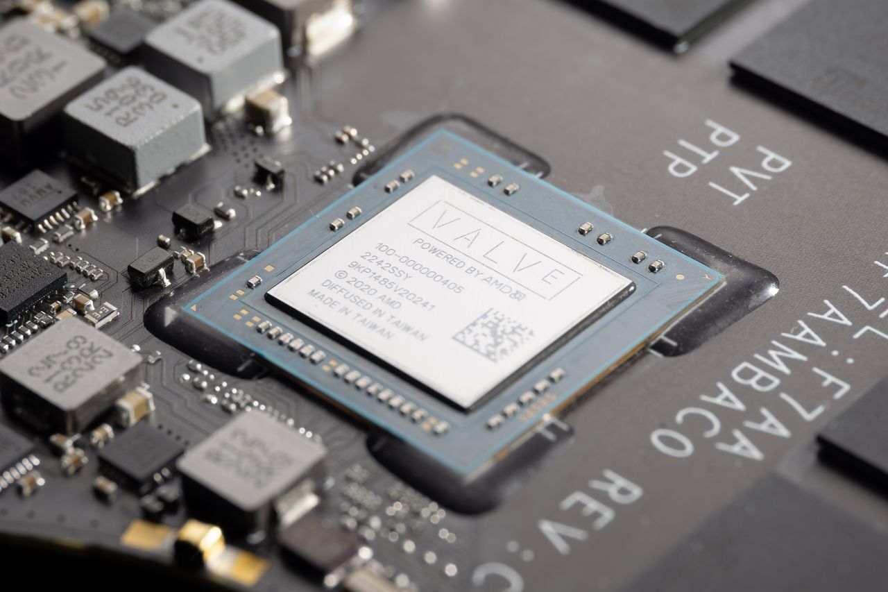
The consoles matter to this series for two reasons. Their volume, tens of millions of chips per generation, is a large part of what has kept AMD's graphics designs funded, as Part 17 described. And they are where AMD is now previewing its next ideas. In October 2025 Sony and AMD described work on what they called radiance cores, which move the tree walk of ray tracing into hardware, and neural arrays, which let neighbouring compute units pool their matrix hardware into one larger engine, both aimed at a console still some years away. Microsoft announced its own next Xbox chip with AMD in March 2026.
RDNA as a home AI machine
Run the same arithmetic Part 21 ran for the RTX 4090. Generating text is memory-bound, so the speed limit is memory bandwidth divided by the bytes of weights read per token, and the size limit is memory capacity. An RX 7900 XTX has 24 GB at 960 GB/s, almost exactly an RTX 4090's, so it holds and runs the same models at roughly the same upper bound: a 30-billion-parameter model at 4 bits, about 18 GB, at up to 50 or so tokens a second. AMD's workstation version of Navi 48, the Radeon AI PRO R9700, sold from October 2025 at $1,299 with 32 GB at 640 GB/s, aimed at people for whom capacity mattered more than speed. For most of these years the larger obstacle was not the hardware but the software, since ROCm, AMD's CUDA counterpart, did not officially support Radeon cards on Windows until a preview in late 2025.
The most interesting AMD chip for running large models at home is not a graphics card. The Ryzen AI Max+ 395, code-named Strix Halo, puts sixteen CPU cores and a 40-compute-unit RDNA 3.5 GPU on one package with up to 128 GB of shared LPDDR5X memory on a 256-bit bus, 256 GB/s. Under Windows up to 96 GB of that can be given to the GPU, more under Linux. A 70-billion-parameter model at 4 bits is about 40 GB, which no single consumer graphics card can hold and this chip holds easily. The bandwidth arithmetic says it will be slow: 256 GB/s divided by 40 GB per token is a ceiling of about six tokens a second, and owners measure around four and a half to five. It is the same trade as Nvidia's DGX Spark: a lot of memory, at a quarter of a graphics card's bandwidth.
What comes after RDNA 4
As I write in October 2026, AMD has not announced a successor to RDNA 4 by name or date. What it has said is that the split of Part 10 is ending. In September 2024 Jack Huynh said that AMD would merge RDNA and CDNA into one architecture for both Radeon and Instinct, which he called UDNA, and in 2026 the data-centre side moved first: the MI455X's compute dies are built from RDNA-style work-group processors running wave32 (Part 30). Reports of the next Radeon's process and timing are rumour so far. The direction is not: one compute unit for both lines, with more matrix hardware and more of the ray tracing in fixed function.
Where this leaves us
RDNA is a study in spending a smaller budget well. Where Nvidia had a wider and faster memory bus, AMD built a large on-die cache to make a narrow bus behave like a wide one, two years before Ada did the same. Where Nvidia built whole ray-tracing engines, AMD did the minimum in hardware and has spent two generations moving more of it there. It tried chiplets in a gaming card, learned that they pay off only at the top of the range, and stepped back to one die and a lower price. And the same compute unit, in smaller and larger doses, runs every current PlayStation, every current Xbox, and the Steam Deck. The matrix hardware arrived late and is now used for the same thing Nvidia uses it for, inventing pixels.
The other thing Ada was the gaming half of was Hopper, the same 4 nm process and nearly the same transistor count spent on a chip with no display outputs at all. AMD's chip of that kind came a year later and is three parts on. First, the third company's gaming cards, and then Hopper itself.
Next: Intel Arc: Intel's graphics cards beside Ada and RDNA, Alchemist's large die and troubled drivers, ray tracing with a unit that sorts rays before shading them, Battlemage doing more with less, and 32 GB cards for running models at home.